

Gallium nitride single crystal in new display applications: microLED technol∏ogy
- Categories:Application areas
- Time of issue:2022-09-26 10:49:58
- Views:0
Description:
Information
- GaN single crystal: smaller size, higher resolution, chip wavelen§gth uniformity, smaller leakage current, higher efficiency under low current drive, homogeneous epi₹taxial MicroLED technology on the road to "Moore's §Law".
 |
 |
WLD=472.5nm,std=0.9nm |
WLD=472.5nm,std=0.9nm |
|
Wavelength uniformity of homogeneous epitaxial chips on GaN single crystal substrates helps to s•olve the massive binning problem and the giant transfer prλoblem. |
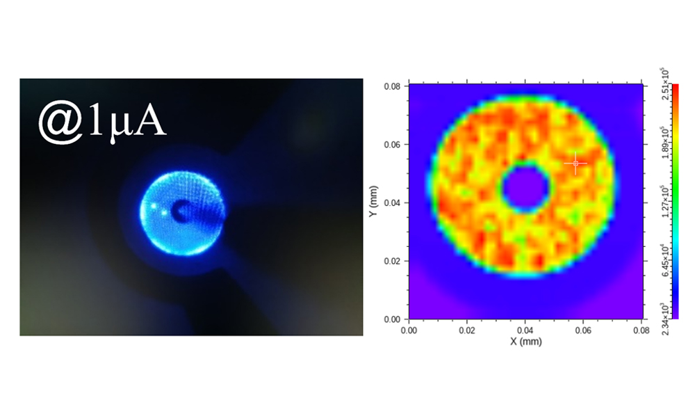
Chips with homogeneous epitaxy on GaN single crystal substrates exhi$bit better luminescence uniformity. |
 |
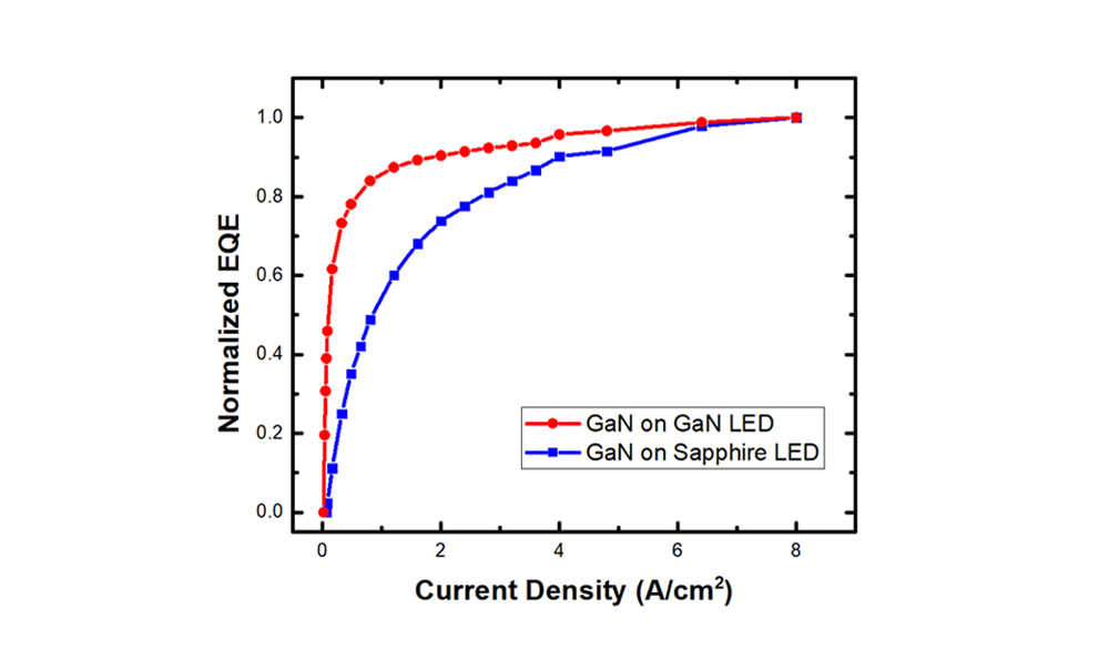 |
| Smaller leakage currents | Higher efficiency with low current drive |
GaN single crystal in new display applications: laser projection displays
- GaN single crystal: GaN single crystal substrate is the only substrate technology for the laser di"splay technology route.
 |
 |
 |
|
VR眼鏡 |
手機(jī)投影(yǐng) |
汽車(chē)顯示 |
 |
 |
 |
| Laser displays | Laser Cinema | Projection |
Contact Us
Add:No.1 Dongdangtian Lane, Suzhou I♥ndustrial Park, Jiangsu Province
Sales Director:
Dai Dongyun: 15962257010
Email: daidongyun@nanowin.com.cn
Sales Assistant:
Miss Ren: 17712482910
Email: renjing@nanowin.com.cn
Online Message
客戶留言
Description:
 159-6225-7010

 Online Inquiry